The
Emperor's New Amplifier TM
by
Norman L. Koren
Updated June 4, 2003
Norman
Koren Vacuum tube audio page | Photography
page
Feedback
and Fidelity | Improved
vacuum tube models for SPICE simulations
November
3, 2002: I've added diagrams
of the hand-wired circuit boards and more footnotes to the main schematic.
February 2003:
Paul
Heggeseth is
building a version of TENA (brave soul). Check his site
for updates.
I spent much of 1997 designing
and building my ultimate dream amplifier, which I named "The Emperor's
New Amplifier"TM (TENA) for a quality it shares with the fabled
emperor's wardrobe-- transparency. It was also an oblique reference to
the marketing hype that pollutes high-end audio. I thought about commercializing
it, especially when the lab where I worked announced it was shutting down,
but I soon realized that marketing high-end tube amplifiers is not a reliable
way to make a living. (I'm paycheck-addicted.) Counterpoint
Electronics, a high-end audio manufacturer located in a 45,000 square
foot building five miles from where I lived at the time, vanished overnight.
Then I thought I might write a magazine article, but the move to Colorado
distracted me.
TENA has been working reliably since 1997,
and in a way it's ruined me as an audiophile. I've become contented. I'm
so pleased with it I've abandoned the quest for audio perfection. (Photography
keeps me busy enough.) Now the time has come to share it-- via the Internet.
Brace yourself for a tour de force of amplifier design. It's arguably
the most sophisticated vacuum tube amplifier ever. But
be forewarned if you plan to build it: It's not a simple project. Absolutely
not for beginners!
Features
-
Output: 4-6550's in triode-mode class AB2
push-pull parallel. About 80 watts RMS per channel.
-
No global negative feedback. Several local
loops with limited negative feedback.
-
Ultra-wide bandwidth Plitron
toroidal output transformer.
-
Servo to maintain precise dc-balance in
the output circuit.
-
MOSFET-regulated power supplies. Relative
rather than absolute voltage reference.
-
Designed using extensive PSpice computer
simulation.
-
Constructed as a pair of monoblocks.
Schematic
diagram
If the schematic diagram is too large to print directly from your Web browser,
save it as a GIF file and print it on an image editor or viewer. If you'd
like to save a larger and more detailed version of the schematic, shift-click
on TENA_Sch_1BIG.gif.
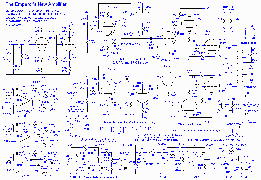
TENA schematic diagram (simplified power supply)
Notes on the schematic diagram
-
The power supply has been simplified-- Power transformers and rectifiers
have been omitted and some parts have been omitted from the MOSFET voltage
regulator circuits: 1N5242 zener diodes between the source and gate and
10k resistors in series with the gate. These parts serve as protection
in case of accidental short circuits, but don't affect the operating point.
The full power supply schematic is shown below.
-
6SN7's are used instead of 12AU7's for the driver tubes. They have the
same plate characteristics, but they have higher maximum plate voltage
(450 vs. 330 V) and greater plate dissipation (3.75 vs. 2.75 W per section).
Think of the octal-based 6SN7 as a 12AU7 on steroids.
-
The NODESET blocks (lower right) initialize dc levels in the bias servo
so the simulation runs properly. They don't exist as physical entities.
-
All resistors are 1/2 watt unless noted, and with the following exceptions.
R3P, R4P and R5C through R8C (68K) are 2W. R9C through R12C (20 ohm) are
1W: I used 2-10 ohm resistors in series to make them. R9S through R12S
(200 ohms) are 2W.
-
Capacitor voltage ratings: It never hurts to go over the minimum, though
the capacitors will be larger and may cost more. I often use caps with
higher voltage ratings because I have them on hand or found them at a good
price in an electronics surplus shop. Here are some minimum ratings: C1G:
100V. C2G: 400V (600V would be better; necessary without the time delay);
C3G and C4G: 400V (600V would be better); C3M and C4M: 400V; C5G through
C8G: 600V; CBS2, CBS4, CBS6 and CBX1 through CBX3: 100V. The voltage ratings
of many of the power supply capacitors are shown on the circuit board wiring
diagrams, below.
-
Some of the feedback connections may be a little hard to trace. ORN goes
between the 20 ohm output transformer secondary feedback winding and R3F
near TU3. Similarly, VLT goes to R4F near TU4. BLU and BLK on the output
transformer secondary speaker winding go to the output tube cathode circuits.
-
RLS (5 ohms) is a simulated speaker load.
-
CRF: All three nodes are connected together.
-
BRN and VIO are not used. They are the ultra-linear taps. In the original
version of TENA there was a switch to select output tube screen grid connections
between BRN and VIO (UL mode) and GRN and YEL (triode mode).
Design
philosophy
In the 1990's I strove to learn the secrets of designing circuits with
superior audio quality. I'm technically curious and also cheap-- I didn't
want to spend big bucks on cosmetically impressive equipment of dubious
design. SPICE computer modeling became my primary learning tool because
it enabled me to observe inner details of amplifier operation not obvious
from outer measurements.
My goal was to design a high-powered wide-bandwidth amplifier with the
finest sound and to keep it simple-- but not too simple. I rejected single-ended
(SE) designs because of their low power and limited bandwidth. I wanted
to see if I could get similar sound quality-- perhaps better-- with an
efficient push-pull design. And I wanted to do it
my way.
I aimed for wide bandwidth, but not too wide. Very low frequency
1/f noise and radio stations don't enhance music. Most of the coupling
circuits have an RC time constant around 0.05 seconds, equivalent to a
-3 dB frequency of 3 Hz-- low but not too low.
No net ac current is drawn from any power supply tap. Pairs of tubes
draw equal but opposite current. This effectively removes the power supply
from the signal path and reduces the need for voltage regulation. Nevertheless
robust MOSFET regulators are employed for ultimate sonic refinement.
I avoid global negative feedback-- a loop from the amplifier
output to its input. There are several local loops-- around one
or at most two gain stages. Local feedback loops have numerous advantages
and no adverse effect on sound quality. Stability is much easier to maintain.
The extreme bandwidth of the output transformer allowed me to put a moderate
amount of feedback in the output circuit while maintaining excellent bandwidth
and stability.
I originally designed TENA to be switchable between triode mode (plate
connected to screen grid) and ultra-linear (UL) mode (plate connected to
output transformer 40% taps). Output modes are discussed in Feedback
and Fidelity, Part 2. In conventional class AB1 operation, UL mode
has much greater output power than triode mode, but it has higher output
impedance and poorer linearity. In class AB2 operation (where grid current
is drawn when the grid is driven positive with respect to the cathode)
I got plenty of power in triode mode, so I eliminated the switch. (Duncan's
Amp Pages has a nice little discussion of operating classes.) A triode
behaves like a pentode with built-in local negative feedback. A
pentode's screen grid suppresses feedback from the plate, but it can be
restored by connecting it in triode mode (connecting the screen grid to
the plate instead of a fixed high voltage). Many audiophiles despise negative
feedback (see Feedback
and Fidelity), but ask them which tube type they prefer...
Try as I might I couldn't keep it simple. Class AB2 operation requires
individual cathode follower drivers, which requires extra power supplies.
So it got complex, but every part has a purpose; none is superfluous. I
did nothing because conventional wisdom told me to.
Components are operated conservatively-- well under maximum power dissipation
and voltage ratings. This ensures maximum reliability.
I tried to avoid exotic, hard to get, or expensive parts. I chose the
6550C over "real" triodes because it's moderately priced, easy to find,
rugged and has high power dissipation. It behaves like a real triode when
connected in triode mode. Most "real" triodes have directly heated filaments
which are difficult to integrate into feedback circuits.
Several aspects of the design philosophy implemented in TENA-- maximizing
stability,
minimizing
RF interference (which can result in"gritty" sound and "listener fatigue"),
and soft
clipping-- are discussed in detail in Feedback
and Fidelity. In writing this article I've become aware of a few things
I may change if I have the time or make TENA into a commercial product,
but I have no such plans at the moment.
Input
stage/phase inverter
Input stage TU1 is a simple voltage gain stage with local negative feedback,
derived from the R1B, R1C voltage divider. It is capacitively coupled to
split load phase inverter TU2. The capacitor has an unusually low value--
0.01 µF-- because TU2 has an exceptionally high input impedance--
several Megohms. The advantage of capacitive coupling is that it allows
the voltage level in TU2 to be set for maximum output and it allows the
ac current in TU2 to be precisely equal to, but 180 degrees out of phase
with, the current in TU1. The net ac current drawn by these two tubes from
V+420 is therefore zero. This is an effective way of isolating the audio
signal from the power supply, which doesn't need to supply ac current.
In conventional designs ac signal often has to flow through electrolytic
capacitors, which are grungy leaky devices with memory-- harmful to audio
quality. I designed TENA to draw zero net ac current from all power supply
outputs (easy to do in a push-pull design), at least up to the power level
where one of the output tube pairs starts cutting off.
Toroidal
output transformer
I chose the Plitron toroidal transformer
because of its exceptional bandwidth: -3 dB at over 200 kHz, the result
of high primary inductance (the good stuff) and low leakage inductance
(the bad stuff-- kind of like HDL and LDL cholesterol)-- much better than
can be achieved with a conventional EI transformer. High bandwidth is important
because output transformers have an intrinsic second order rolloff, which
can make them unstable in the presence of negative feedback unless careful
phase compensation is applied (see Feedback
and Fidelity). Phase compensation reduces the bandwidth, which is not
a problem with the Plitron toroidal transformers. But this bandwidth comes
at a price-- toroidal transformers are much less tolerant of dc-imbalance
than EI transformers; they may saturate at dc imbalances as low as 8 mA.
(I don't know the exact number; I never simulated it.) You would have to
set the bias of each tube individually, and then you'd have to worry about
how the tubes age. So I designed a bias servo circuit to maintain perfect
dc-balance under all circumstances except outright tube failure.
The Plitron PAT 4006CFB 100 Watt toroidal output transformer is not
currently listed on Plitron's website, but I've heard (June 2003) that
it is available. Contact Norman Woo.
The closest models are the 4006, which lacks the special feedback winding,
and the 2100-CFB which has a higher primary impedance. The minimum feedback
version of TENA
(below) works with the 4006.
I won't go into detail about modeling toroidal transformers-- Plitron
has a treasure
trove of fine articles on its Website, and I said a few things
in Improved
SPICE models.
Bias
servo and adjustment
The time-averaged (low pass filtered) dc current of an output tube operating
in class AB fixed bias is relatively constant at low power levels but increases
at high power levels. For this reason a fixed voltage cannot be used as
a reference for biasing the output tubes. One tube (TU9, driven by TU5)
operates at fixed bias, and its low pass filtered cathode voltage (CRF)
is used as the reference for biasing the other tubes.
The bias servo is illustrated in the lower left of the schematic. It
uses the LM324 quad op amp-- cheap but perfectly adequate. Inputs U1A,
U1B and U1C of the LM324 compare cathode voltages 10C, 11C, and 12C with
reference voltage CRF, which is the voltage on cathode 9C low pass filtered
with RBS2 = 33k and CBS1 = 10µF ( located near U1B on the schematic).
The LM324 outputs control the P-channel MOSFETs, each of which controls
a voltage divider between VBB (-90V) and VOP (+12.5V) to deliver the appropriate
bias voltage to the driver grid circuits (BIAS_6, BIAS_7, and BIAS_8).
This measures between -45 and -50V in my amplifiers, which operate at 60
mA plate current. Audio purists please note: the servo operates at extremely
low frequencies; the op amp and MOSFETs are well outside the audio signal
path.
A single potentiometer, RB5 (in the VBB supply, bottom center), controls
the bias current directly in TU9, and all the other tubes indirectly through
the servo. Bias current may be measured across any of the 20 ohm resistors
R9C-R12C as E/20. They should all be the same if the servo is working
properly. 1 to 1.2 volts is a good nominal value, corresponding to 50 to
60 mA per tube (70 mA was used in the Dynaco Mark III). Increasing the
current increases power consumption and reduces tube life and output power,
but moves you closer to Class A (where both tubes always conduct).
Feedback
The main feedback loop goes from the 20 ohm cathode
feedback winding on the output transformer secondary (ORN, VLT) to the
cathode circuits of the second gain stages, TU3 and TU4. This is a much
shorter path than a typical feedback loop, which returns to the first input
stage, and it is also balanced. Resistors R3C and R3F on the cathode of
TU3 and R4C and R4F on the cathode of TU4 form a voltage divider than determines
the amount of feedback-- about 12 dB for the output stage in triode mode.
The feedback loop is stabilized by 15pF Miller capacitors C3M and C4M.
This is a much better approach than the common technique of putting the
stabilization capacitor(s) in parallel with the feedback resistor(s), which
feeds RF signals picked up by the speaker wires back into the input stages.
This issue is discussed extensively in Feedback
and Fidelity. Output is virtually unchanged with 1µF is placed
in parallel with the 5 ohm loudspeaker RLS.
The cathodes (including the feedback winding center
tap WHT) are referenced to VBB = -90V. This gives TU3 and TU4 the huge
voltage swing required for the zero-gain cathode followers that drive the
triode output stage. The large voltage swing is the reason that the 6SN7
was chosen over the 12AU7, which has a similar plate curve. If the output
stage were operated in ultra-linear mode, it would have higher gain and
wouldn't require as large a voltage swing on TU3 and TU4.
There is also a lesser feedback loop between the
speaker windings (BLU, BLK) and the output tube cathodes. This loop provides
less than 2 dB of feedback-- a very small amount. If I were an anti-feedback
purist, I'd eliminate the main loop (to the cathodes of TU3 and TU4) as
described below, but I'd keep this one, which qualifies
as a local feedback loop because it involves only one amplification stage--
the output stage.
Class
AB2 output stage and drivers
Class AB2 differs from the more common class AB1 in that the output stage
grid is driven positive-- it draws grid current-- at high power levels.
Class AB2 has no advantage for output tubes operating in pentode mode and
little advantage for ultra-linear mode. But it results in a huge power
boost for output tubes operating in triode mode. You can get almost as
much power out of class AB2 triodes as you can out of class AB1 pentodes.
If you try to do operate in class AB2 with conventional capacitive coupling,
the coupling capacitor starts charging as soon as grid current is drawn.
This drives the grid negative-- toward cutoff, and it recovers with the
RC time constant of the coupling capacitor and grid resistor. To operate
successfully in class AB2, the output stage must be either transformer
or direct coupled. I chose direct coupling because interstage transformers
are expensive and have limited bandwidth.
The direct coupled drivers are the source of much of TENA's complexity.
Because the quiescent grid voltage of each output tube must be set individually
to control its quiescent (dc) current, one driver tube (TU5-TU8) is required
for each output tube (TU9-TU12). Cathode followers (CF's) were chosen because
they have low output impedance and can source the needed output tube grid
current. The cathodes have to be somewhere near -50V to properly bias the
output tubes. This means the CF must be driven by voltages outside the
range of conventional power supplies, hence the need for VDR- and VDR+:
the price of perfection. In reviewing the design I find that the driver
tubes may be operating a little too conservatively-- dissipating
only 0.78 W (of a 6SN7 maximum of 3.75 W). I've discussed driver dissipation
under PSpice output, below. I may increase VDR+ from
205 to around 250 V by increasing RD1 from 470k to 680k. This would reduce
the power dissipation in MOSFET MD1.
Output tube grid stop resistors R9G-R12G play an important role in TENA's
soft clipping. When power levels become high enough level for grid current
to be drawn, a voltage drop across these resistors gradually limits the
plate current. Soft clipping consists of low order harmonics which have
much less adverse effect on sound quality that the high order harmonics
characteristic of abrupt clipping. But total harmonic distortion for soft
clipping amplifiers tends to be higher. Yes, lower harmonic distortion
doesn't mean better sound. See "The great harmonic distortion scam" in
Feedback
and
Fidelity. TENA oscillated when the grid stop resistors were removed.
This was the only performance feature PSpice didn't catch. The reason
is that the output transformer model is somewhat simplified-- it's extremely
difficult to model its distributed capacitance.
Power
supplies
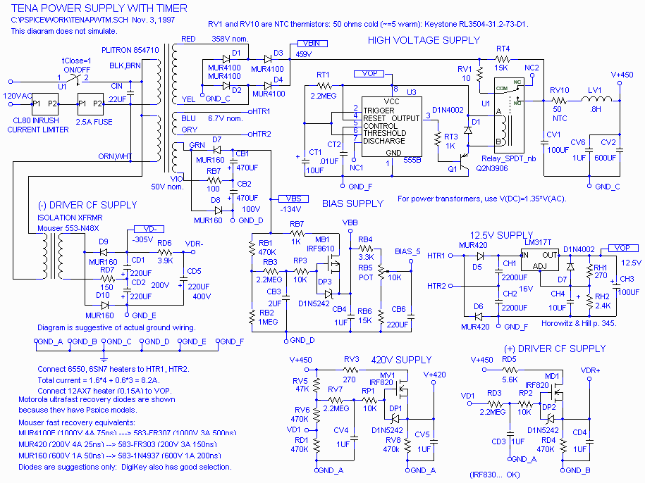
Power supply detail
The time delay circuit (U3
(the 555B chip), Q1, Relay_SPDT_nb,
RT1, CT1, CT2, RT3, D1, RV1, and RT4) has apparently never been implemented.
RT4 should be replaced by a straight wire; VBIN is connected directly to
NTC (negative temperature coefficient; 50 ohms cold; Mouser527-3504-50)
thermistor RV10.
The precise values of most of the capacitors in
the power supply, particularly CV1, CV2, CB1, CB2, CD1 and CD2, are not
critical. In many cases they were determined by parts availability. If
the values are 2 uF or under they are film capacitors. If they are over
2 uF they are electrolytics.
Depending how you count there are two (power transformers),
four (rectifier circuits) or six (voltage levels). All use fast recovery
rectifier diodes. All except VDR- are taken from the mighty Plitron 854710
toroidal power transformer, which I can't seem to find in their catalog.
Toroidal power transformers perform well, but they have less of an advantage
than toroidal output transformers-- you don't need wide bandwidth for 60
Hz. The CL80 inrush current limiter limits turn-on current in the tube
filaments.
NAME
Location |
POWER SUPPLY
DESCRIPTION |
V+450
Top |
Main high voltage supply for output tubes (TU9-TU12).
About 450V unregulated. Uses 4 MUR4100's in a bridge. NTC thermistor RV10
(Mouser527-3504-50)
limits relay turn-on current. Uses two large filter capacitors CV1 and
CV2 and choke (inductor) LV1. V+450 is the input to V+420V and VDR+. [
A circuit employing a 555 timer was designed to delay turn-on for about
20 seconds, giving tube cathodes time to warm up. The intent was to prevent
a turn-on voltage surge which could potentially damage components such
as filter and coupling capacitors. RT4 allows the supply voltage to gradually
build up before the relay turns on. This protects the relay contacts by
reducing the transient turn-on current. Its value (15k) was not highly
optimized. In November 2002 I examined TENA, and found that the time delay
circuit had never been implemented. Reliably is fine without it. Amazing
what I've forgotten since 1997. ] |
V+420
Bottom center |
420V regulated supply for input stages (TU1-TU4).
Could be considered part of the main high voltage supply. Regulated by
IRF820 N-channel MOSFET with a modest heat sink. |
VDR+
Bottom right |
Positive supply for driver tubes (TU5-TU8). About
200V. The IRF820 N-channel MOSFET regulator is controlled by a voltage
divider (RD1, RV6) in the 420V supply. Requires a substantial heat sink.
In reviewing the design I see it might be slightly perferable to to source
VDR+ from V+420. |
VDR-
Center left |
Negative supply for driver tubes (TU5-TU8). About
-305V. Uses a separate isolation transformer (1:1 voltage ratio)
with a voltage doubler. Unregulated. |
VBB
Center |
-90V negative bias supply for output tubes, also
connected to TU3 and TU4. Uses voltage doubler taken from power transformer
bias winding. Regulated by IRF9610 P-channel MOSFET with a modest heat
sink. |
VOP
Center right |
12.5V regulated supply for bias servo. Uses voltage
doubler taken from filament winding and LM317T regulator. |
I tried and failed to keep it simple, but the
sophisticated power supply is one of the keys to TENA's superb sound quality.
MOSFET
regulators
Thanks to Dennis Lusis for teaching me this technique.
A MOSFET (Metal Oxide Semiconductor Field Effect Transistor) is a three
element device whose terminals are a source, a drain, and an infinite impedance
gate, shown respectively on the bottom, top, and left of the MOSFETs in
the schematic diagram. You may think of the common N-channel MOSFET (IRF820
in TENA) as a valve that maintains the source at a constant voltage (between
1 and 2 volts) below the gate as long as the drain is several volts higher.
The less common P-channel MOSFET (IRF9610 in TENA) has the opposite polarity--
the source is maintained at a voltage above the gate. At high frequencies
this picture is mucked up by gate capacitance.
The 420V supply (V+420) on the bottom of the power
supply schematic is a good example. Output voltage (V+420) is controlled
by the gate of MV1-- set by the RV5, RV6+RD1 voltage divider and the RV7,
CV4 low pass filter. RV7 can have a very high resistance (2.2 Megohms)
because the gate has infinite impedance. This allows the use of a film
capacitor instead of a leaky, noisy, unreliable electrolytic for CV4. When
I hooked TENA to a pair of extremely efficient loudspeakers (normally driven
by SE triodes), I heard a very slight hum. Because of this I would consider
redesigning the low pass filter in two stages (adding an R and C) for a
future iteration of TENA.
The primary function of voltage regulators is
to maintain constant supply voltage independent load current. They are
particularly useful when a large voltage drop is required, as in the VDR+
supply, which drops over 400V to 200V. TENA uses
relative rather
than
absolute regulation. The reference for a relative regulator
is a multiple of the line voltage. It it's done well, the reference voltage
will change slowly and without transient noise in response to changes in
the line voltage. An absolute regulator requires a fixed voltage reference.
High voltage fixed references, suitable for vacuum tube circuits, have
their share of problems. For example zener diodes can be plagued by noise
and temperature coefficient issues. Since the amplifier's gain is hardly
affected by the supply voltage, I prefer relative regulation; I know
of no disadvantages. It's simple, reliable and quiet. Some other
MOSFET regulator designs can be found in Duncan's
Amp Pages and the Mods section of Welborne
Labs' catalog.
Minimum
feedback modification
 Since
triodes have low enough output impedance to drive most loudspeakers without
negative feedback, it's tempting to look at how TENA would perform with
the main negative feedback removed-- without the feedback from the secondary
cathode feedback widing (ORN, VLT) to the cathode circuits of TU3 and TU4.
Feedback can interact with difficult loads in nasty ways. Even though TENA
has been designed for extreme stability-- response is virtually unchanged
with 1 µF in shunt with the loudspeaker-- I haven't looked at every
possible difficult load, like inductive loads. And of course many audiophiles
dislike the audible effects of feedback (perhaps because it's often implemented
badly).
Since
triodes have low enough output impedance to drive most loudspeakers without
negative feedback, it's tempting to look at how TENA would perform with
the main negative feedback removed-- without the feedback from the secondary
cathode feedback widing (ORN, VLT) to the cathode circuits of TU3 and TU4.
Feedback can interact with difficult loads in nasty ways. Even though TENA
has been designed for extreme stability-- response is virtually unchanged
with 1 µF in shunt with the loudspeaker-- I haven't looked at every
possible difficult load, like inductive loads. And of course many audiophiles
dislike the audible effects of feedback (perhaps because it's often implemented
badly).
Removing this loop would increase TENA's gain
a bit much, so I apply local feedback (the good kind with no adverse side
effects) to the cathode circuits of TU3 and TU4. To eliminate the main
feedback loop, remove all conections from the output transformer secondary
cathode feedback winding (ORN, VLT) and remove C3M and C4M. Reconfigure
R3C and R3F as shown on the right. Changes to TU4 should exactly mirror
the changes to TU3.
I haven't tried this yet. I'll report on it if
and when I do. Simulated frequency response is virtually unchanged. One
significant advantage: You can use the Plitron
PAT 4006 output transformer, which is a part of their current product
line.
Simulated
performance
Actual measurements are very close to the simulations,
but simulated measurements are much easier to display on a Web page.
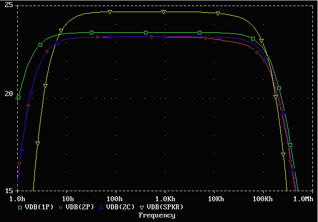
PSpice simulated TENA frequency response in dB at TU1 plate (1P;
green),
TU2 plate and cathode (2P and 2C; red, blue), and Speaker (SPKR;
yellow)
Few tube amplifiers come close and none get better-- 1 dB down (±0.5
dB) at the output (SPKR) at 9 Hz and 80 kHz with no irregularities at any
of the intermediate stages. Perfect match between phase inverter outputs
below 10 kHz. No more than 0.2 dB difference above 20 kHz. Response is
stable even under difficult loads. A 10 kHz square wave has only a slight
overshoot and no ringing when TENA is loaded with a 2 uF capacitor (a similar
load to a large electrostatic speaker) in parallel with a 5 ohm resistor.
Most competitive "high-end" amplifiers show severe ringing under these
conditions.
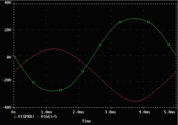
PSpice simulated TENA time-domain response at driver grid (divided
by 5; red) and output
(SPKR; green), driven hard enough to illustrate soft clipping, which
starts at V(SPKR) = 24V,
equivalent to 116 Watts Peak = 58 Watts RMS into the 5 ohm speaker
load.
The PSpice model for soft clipping is rather crude; actual onset is
more gradual than the simulation indicates. Below 57 Watts RMS, distortion
is vanishingly low. It increases gradually above 57 Watts, but is of very
low order. That's why I tell people the output is "about" 80 Watts RMS.
The advantage of a design with gradually increasing low order distortion,
as opposed to an extremely linear design that clips abruptly, is discussed
in Feedback
and Fidelity.
Output impedance is around 0.9 ohms. The power output and damping factor
are sufficient to drive nearly any loudspeaker.
Sound
quality
I've read enough hyperbole about amplifier sound quality to sink the Titantic
without the benefit of an iceberg. So I'll simply say it sounds wonderful--
extremely clear and dynamic. It's everything I expected, though it's not
as "sweet" as single-ended amplifiers, which benefit from rather large
amounts of second harmonic distortion. The quest is over. I have other
windmills to tilt (photography). Fair Dulcinea awaits.
Norman
Koren Vacuum tube audio page | Photography
page
Feedback
and Fidelity | Improved
vacuum tube models for SPICE simulations
Additional
notes
I used point-to-point wiring on several perfboards:
neither beautiful nor manufacturable, but TENA has worked flawlessly since
1997. I would have designed a PC board (actually, several) if I'd had the
time to learn how. They're the only way to go for manufacturability and
they're also prettier, which is vital for marketability. I used polypropylene
capacitors throughout the audio path. I didn't experiment with exotic capacitors
or resistors. If you're interested in the sonic effects of capacitors,
check out Bob Pease's article on "Soakage"
in capacitors. The chassis was from Mark V Electronics in Los Angeles,
now sadly out of business. Size is 2 3/4x19"
(approx. 7x48 cm) for the front panel
and 2.5x17x12"
(approx. 6.3x43x30.5
cm) for the main chassis.
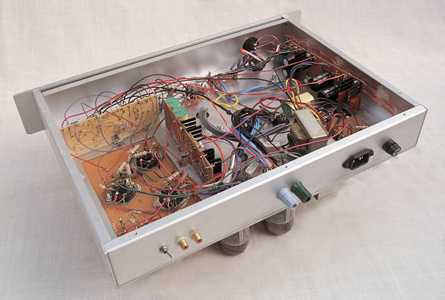
TENA has three hand-wired perfboard circuit boards (Radio Shack 276-1395).
PC boards would be preferable, but the perfboards have been reliable. The
scales are in inches. The drawings were done in Corel Draw, which probably
isn't ideal, but it was on my computer and I knew how to use it. The illustrations
show the component side of the boards. The wiring on the opposite side
is shown as thick gray lines. When I built thems I printed out these diagrams
along with mirror images so I could see the wiring side in the proper orientation.
The ruler shows inches.
GND is ground.
The original Corel draw files can be downloaded by shift-clicking on TENAboards.zip.
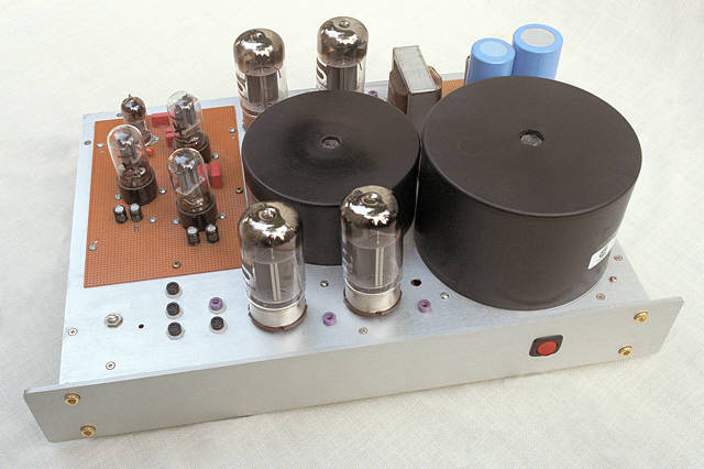
BIAS SERVO
BOARD The wiring side is visible on the left
in the photograph, above. The socket is for the LM324 op amp. 3 IRF9610
MOSFETs are used (the GDS rectangles). POT
is RB5. The zener diodes (Znr),
not shown in the schematic diagram above, protect the MOSFETs and IC against
static electricity events. The type is not critical. The 1N5242 works fine.
They were omitted because they have no effect on the normal operation of
the circuit; they would only complicate the simulations.
POWER SUPPLY
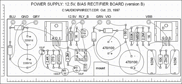
VOP, VBB, TIME DELAY BOARD The component side
is visible on the right in the photograph, above. GRN
and VIO are the bias secondary of the
power transformer, about 50V RMS. BLU
and GRY are the heater windings of
the power transformer secondary. (I think the schematic should have shown
6.3V instead of 6.7V.) The 12.5V pin
is VOP. RLY_B
goes to the relay that delays the turn-on of the high voltage supply. I
apparently changed RB1 from 470k (in the schematic) to 330k. An LM317T
voltage regulator (AOI) and an IRF9610
MOSFET (GDS), both on small heat sinks,
Mouser532-504102B00,
is used. The socket is for the 555B timer, which
has been omitted in the version of TENA I built, along with its associated
circuitry (parts close to the RLY_B
pin: 1N4002, Q1 (EBC), 2.2M, 1K, 10UF, .01).
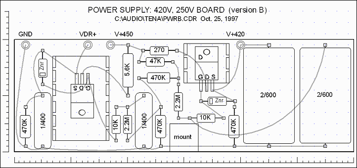
POWER SUPPLY
+420V, +250V BOARD The wiring side (mostly)
is visible near the middle of the photograph, above. 2 IRF820 MOSFETs,
mounted on heat sinks (a large one, Mouser532-551002B00,
for MD1, on the left, which must drop a large voltage), are used. 470K
resistors RV6, RD1 and RD4 are rated at 1W.
PSpice
output
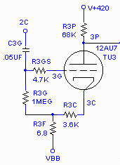
This portion of the PSpice ASCII output file shows voltages at key nodes.
By knowing resistances between nodes, current can be calculated from Ohm's
law. For example, the cathode resistor for one of the driver tubes, R5C
= 68K, is connected between VDR- and 5C. The voltage drop across the resistor
is -49.68-(-257.36) = 207.68 V. The current is I = V/R = 3.05 mA. The power
dissipation in this resistor is P = VI = V2/R = I2R
= 0.634 Watts. So I use a at least a 1 watt resistor, with 2 watts recommended.
The voltage drop across the 6SN7 tube is VDR+ - V(5C) = 204.9+49.7 = 254.6
V. The power dissipated by the 6SN7 is VI = 254.6*0.00305 = 0.78 watts.
The 6SN7 is operating extremely conservatively: Maximum plate dissipation
per plate with both operating simultaneously is 3.75 watts. Maximum DC
plate voltage is 450 V. A 12AU7A would have worked fine: its maxima are
2.75 and 330. I may boose VDR+ to 250 V to give the drivers a little extra
oomph.
**** SMALL SIGNAL BIAS SOLUTION
TEMPERATURE = 27.000 DEG C
NODE VOLTAGE NODE
VOLTAGE NODE VOLTAGE
NODE VOLTAGE
( 1C) 9.0105 ( 1G)
7.6727 ( 1P) 235.3900 ( 2C)
109.9600
( 2G) 108.6600 ( 2P)
302.9800 ( 3C) -70.1920 ( 3G)
-82.5550
( 3P) 179.6100 ( 4C)
-70.1920 ( 4G) -82.5550 ( 4P)
179.6100
( 5C) -49.6790 ( 5G)
-62.7190 ( 6C) -49.6930 ( 6G)
-62.7340
( 7C) -49.6930 ( 7G)
-62.7340 ( 8C) -49.6930 ( 8G)
-62.7340
( 9C) 1.1049 (
9S) 438.3000 ( 10C) 1.1033 (
11C) 1.1033
( 12C) 1.1033 ( 12S)
438.3000 ( A_6) 1.1080 ( A_7)
1.1080
( BLK) 0.0000 ( BLU)
0.0000 ( BRN) 438.6700 ( B_6) -62.7350
( B_7) -62.7350 ( B_8) -62.7350
( CRF) 1.1094 ( GRN) 438.6700
( INP) 0.0000 ( ORN)
-82.5560 ( VA6) 6.6810 ( VB2)
-102.4900
( VB3) 435.7900 ( VB4) 367.8200
( VB6) 10.5180 ( VBB) -82.5560
( VBS) -115.0000 ( VD-) -305.0000 (
VD1) 208.8900 ( VIO) 438.6700
( VLT) -82.5560 ( VOP) 12.5000
( YEL) 438.6700 ( SPKR) 0.0000
( VBIN) 446.0000 ( VDR+) 204.9200 ( VDR-)
-257.3600 (V+420) 413.8200
(V+450) 438.6700 (BIAS_5) -62.7190 (BIAS_6) -62.7350
(BIAS_7) -62.7350
(BIAS_8) -62.7350 ($N_0001)
7.6727
($N_0002) 7.6723
Norman
Koren Vacuum tube audio page | Photography
page
Feedback
and Fidelity | Improved
vacuum tube models for SPICE simulations
.
This page
created
December 8, 2003 |
Images
and text copyright (C) 2000-2012 by Norman
Koren. Norman Koren lives in Boulder, Colorado. Since 2003 most of his time has been devoted to the development of Imatest. He has been involved with photography since 1964.
Designing vacuum tube audio amplifiers was his passion between about 1990
to 1998. |
 |